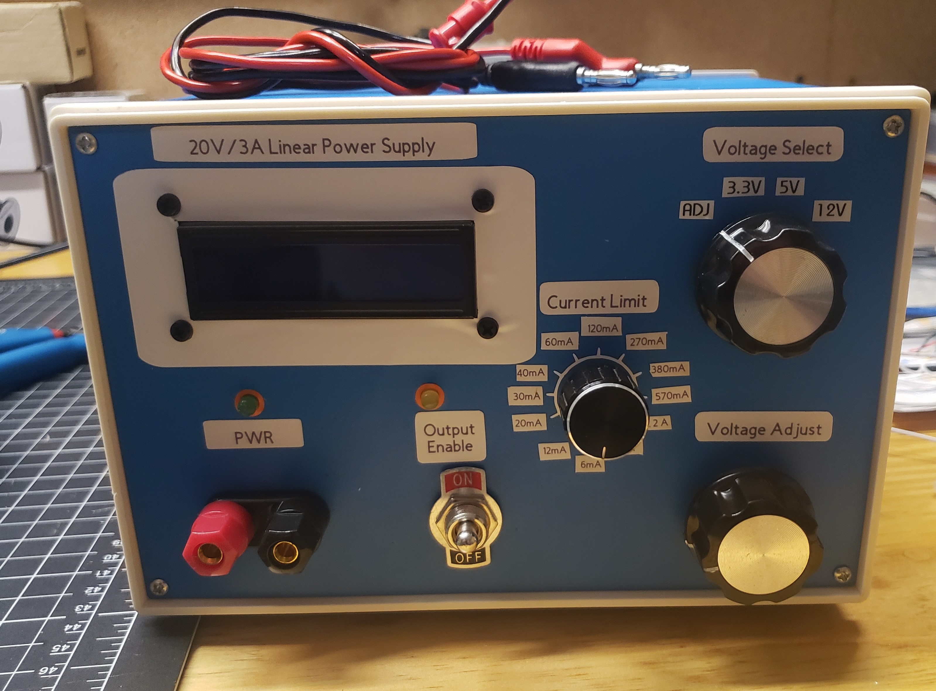
Linear Lab Power Supply
A design and build guide of a lab bench power supply.
Introduction
The purpose and goals of this project are to become familiar with linear power supply design, prepare engineers to transform, regulate, and rectify power for future projects, and create a critical tool for any engineer’s lab.
Power transformation, AC‑to‑DC rectification, and voltage regulation are key components for practically every electrical project. With this project, we aim to design a 20 V/3 A linear power supply with adjustable voltage and current‑limiting capability. We also aim to create a precise voltmeter and ammeter to relay the status of the supply.
Methods
Note
The project draws from numerous engineering concepts. For general reference and theory, concepts and components from the pages below are employed. Topics that required greater detail for clarification are revisited.
Project Overview
This linear power supply aims to provide up to 20 V at 3 A. The design employs linear regulators to minimize noise of the output, adjust voltage, and provide a current limit for the device. The power supply will need to be monitored for the output current and voltage. A Raspberry Pico will be employed for taking voltage and current measurements and displaying them on an LCD for the user. LED indicators, reverse‑polarity protection, and output enable switch are also added for a better user interface. A fuse will also be used for the safety of the user and the device.
Introduction to AC/DC Linear Power Supply
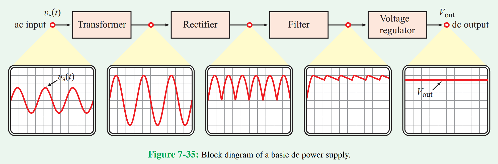 Fig 7-35 of Circuit Analysis and Design1 Block diagram of a basic AC‑DC linear power supply
An AC‑to‑DC converter can be broken up into multiple stages. An AC input usually needs transformation of the existing power to step up or down voltage to the desired range of operation. In our case, 120 V wall power needs to be stepped down by a factor of six to eight before use in the rest of our circuit. This will bring the AC voltage of the secondary between 15 and 20 V, ready for rectification from AC to DC. A full bridge rectifier is employed to have current flow in the same direction for each half cycle of the AC wave. A rectified wave would then require filter components for reducing voltage swing. Capacitors are employed to store change and mitigate this voltage swing, but a separate step for regulation is required. Regulation can be accomplished using multiple methods, primarily using voltage regulator ICs or Zener diodes in reverse breakdown.
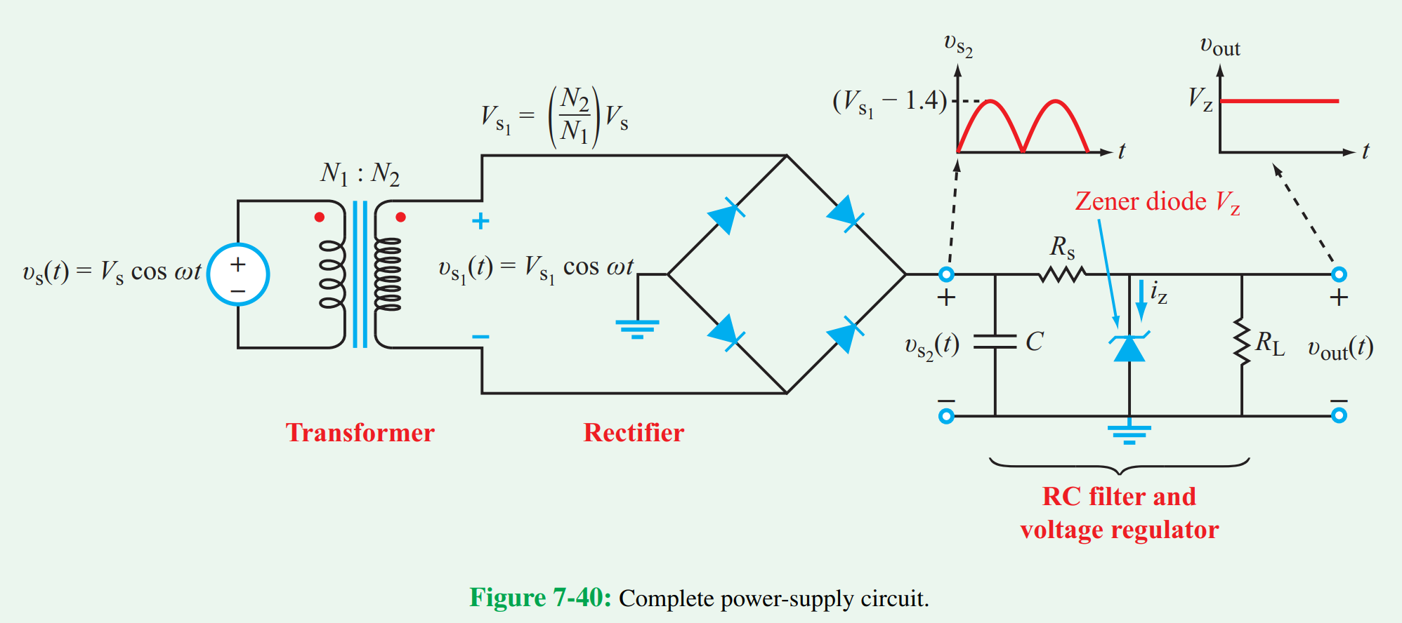 Fig 7-40 of Circuit Analysis and Design1. Complete circuit of a basic power supply using a zener diode regulator
Power Supply Circuit Design
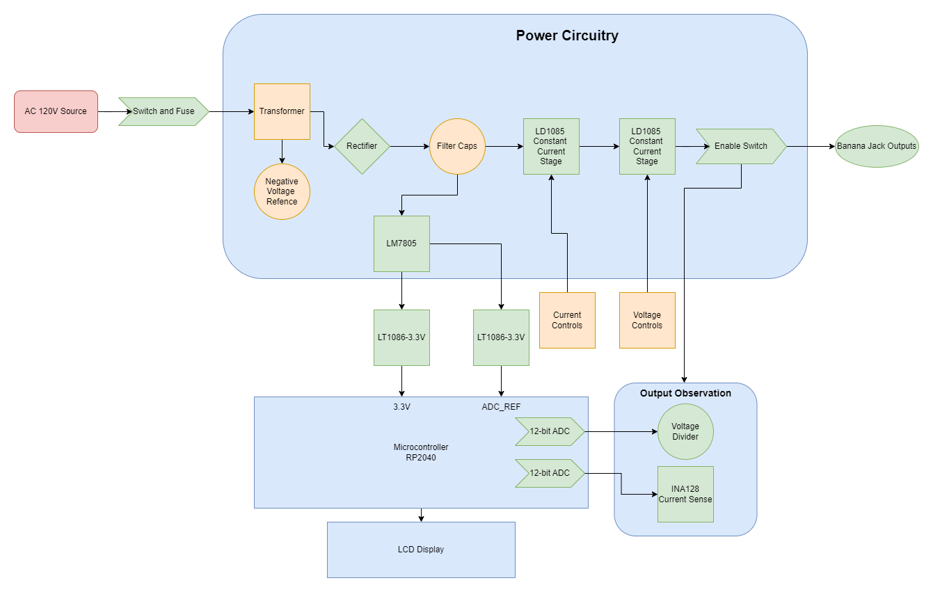 Hardware Block Diagram of the Linear Power Supply
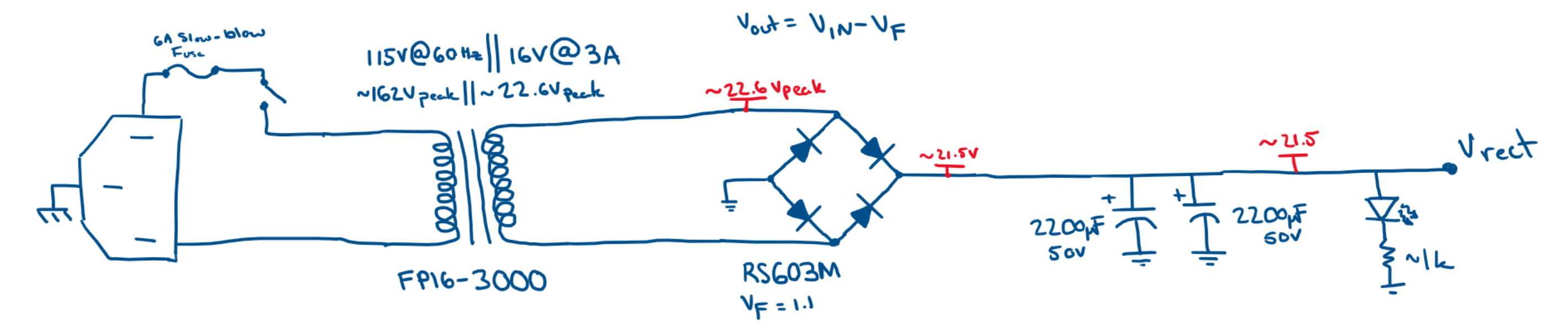
The circuit implements the general systems shown in the block diagram. From the AC outlet, a fuse and switch connect mains voltage to the device for operation. The Flat‑Pak 16 V transformer (FP16‑3000) can deliver 48 VA of power. This device is perhaps one of the most limiting factors of the supply. I anticipate 22.6 V peak‑to‑peak voltage from a 115 V AC circuit, which may not be enough for a 20 V output after regulation. This will be followed by an RS603M full bridge rectifier, with a forward voltage drop of 1.1 V. Two 2200 µF capacitors follow the rectifier for filtering, providing a raw DC voltage around 21.5 V to the following circuit stages.
 Input voltage conditioning stage
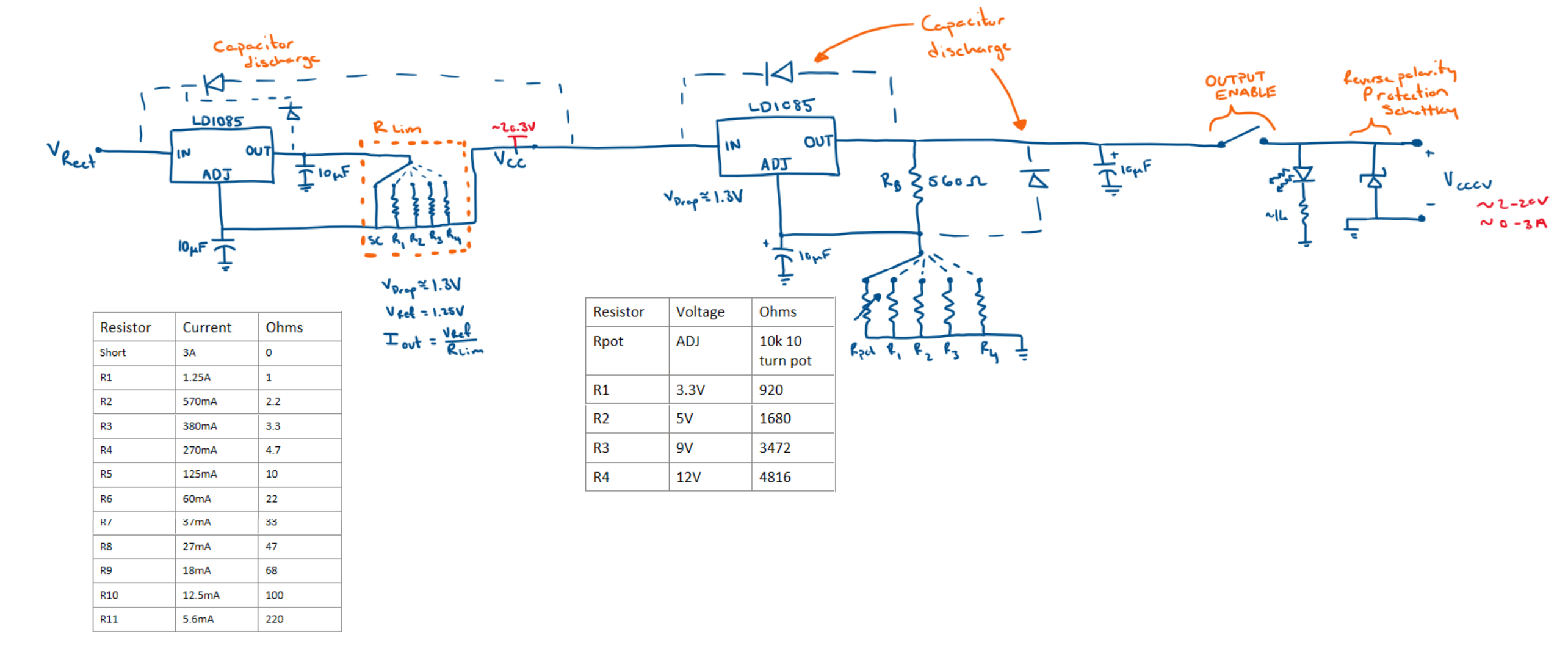
The rectified voltage is passed into the Constant Current Constant Voltage (CCCV) stage for output conditioning. Both stages center around an LD1085 linear regulator IC, which has a 30 V rating and can supply 3 A of current. The constant current stage uses a selection of switchable series resistances to determine the current limit of the following stage. Both output and adjust pins are bypassed for better noise performance but this comes at the cost of storing and possibly supplying more energy during a transient spike from the load.
The constant voltage stage allows for switching between a selection of fixed voltage outputs and an adjustable output. Given there is no current limiting occurring, the device should provide 1.25 V to about 20 V. The output’s upper boundary is limited by the dropout voltage over both linear regulators, forward voltage of the rectifier, output of the transformer, and the AC voltage seen at the plug. The supply should comfortably hit 20 V on the output under moderate loads; however, bottlenecks may be encountered for worst‑case scenarios. Again, each terminal of the LD1085 is bypassed for noise performance. Diodes are incorporated for protection purposes on each regulator and will provide a discharge path for capacitors on the adjust and output pins when the device is turned off. An output enable switch, reverse polarity diode, and an LED are employed for output safety and interaction.
 Constant Current‑Constant Voltage Stage with reverse polarity protection
Warning
There are some flaws with the constant current circuit as depicted. Decoupling capacitors on the output and adjust pins of the constant current regulator cause current spikes from various operations. The short circuit implemented originally was removed in favor of a 0.33 Ω resistor providing the same effect as before. Finally, to reduce transient uncertainty when switching between Rlim resistors, a 10 kΩ resistor was added in parallel to Rlim.
If you attempt to recreate this constant current circuit, remove the decoupling capacitors, short circuit condition, and add a high resistance in parallel to Rlim.
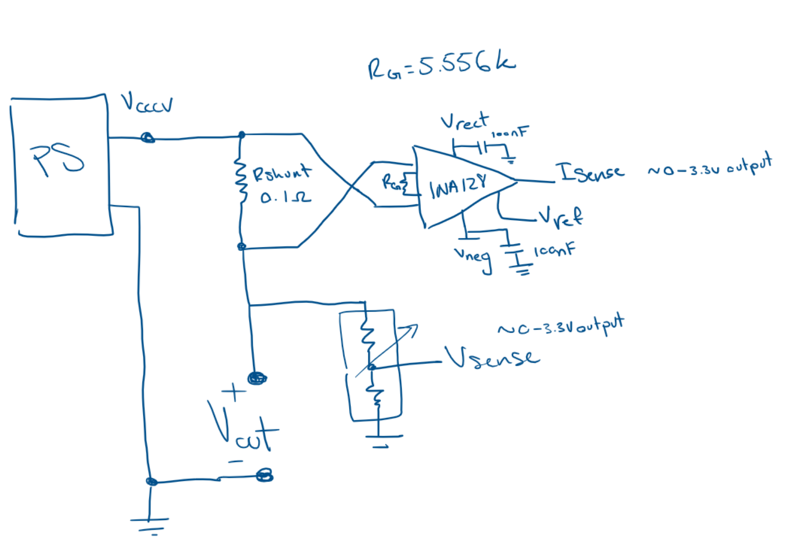
The output of the CCCV then feeds into the measurement circuitry for observation and user interaction. A 0.1 Ω shunt resistor is added for high‑side current sensing. This was done with the INA128 which should have no problem observing the dynamic range of the power supply. The current can be no more than 3 A as set by both the transformer and the regulators. This circuit observes currents in the full operation range and imposes minimal voltage loss on the output. A 100 W rated shunt is used for safety during a short‑circuit condition. A gain of 10 is applied to make the output voltage functionally equivalent to the observed current over the shunt resistor. This means that a 0–3 V output can easily be read by a 3.3 V ADC. The output voltage is observed through a resistor divider that similarly creates a 0–3 V output for ADC readings. The ratio of loss from the divider is inverted and applied back to the sensed ADC value in software to relay the correct output voltage.
 Input voltage conditioning stage
The INA128 used for current readings has a 36 V operation range and requires about 2 V of offset from each rail to operate effectively. The device will be supplied by both the rectified voltage and a negative reference voltage. This is because the rectified voltage should be approximately 2 to 3 V higher than the output of the voltage regulator, giving enough room for higher voltage measurements. However, the device must also output on the 0–3 V range. To do this effectively, a negative voltage reference must be made to supply an offset from the lower rail of operation. A negative voltage rail around –3 to –7 V is sufficient. This was done using a negative voltage charge pump that feeds a VBE multiplier, giving a nice output reference. The INA128 will only draw about 1 mA of current from this rail, so a charge pump is fine for this purpose.
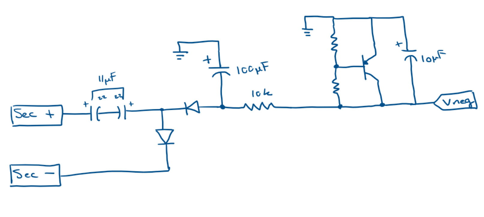 Negative voltage charge pump with VBE multiplier output
Pico Setup
To supply power to the measurement devices, I chose a combination of regulators to power the sensor devices. This provided a smooth 5 V and 3.3 V source for most components, with local decoupling capacitors where needed. The LM7805 is a prime candidate for 5 V regulation as its implementation is simple, only requiring two capacitors on the Vin and Vout. The 7805 is also tolerant to the range of voltage seen after rectification.
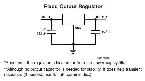 Fixed Output Regulator configuration for an LM7805
In addition to the 5 V source, I powered the Raspberry Pico via 3.3 V regulators. Two 3.3 V rails were also developed using LT1086 regulators, also in a fixed configuration. One regulator was connected directly to the 3.3 V rail, while the other was connected to the ADC reference.
 Pico Power‑chain
ADC Configuration
 Pico ADC reference circuit
For this project, I did everything I could to isolate the ADC reference for the best possible readings. Essentially, I have added a separate 3.3 V linear regulator specifically for the ADC reference. To use this reference voltage without digital operation or SMPS noise, I have removed the R7 resistor that connects the Pico’s 3.3 V source to the ADC reference. This method heavily isolates the ADC reference. It is potentially overkill, but I was interested in seeing how the device would perform.
Pico Software
 Hardware Block Diagram of the Linear Power Supply
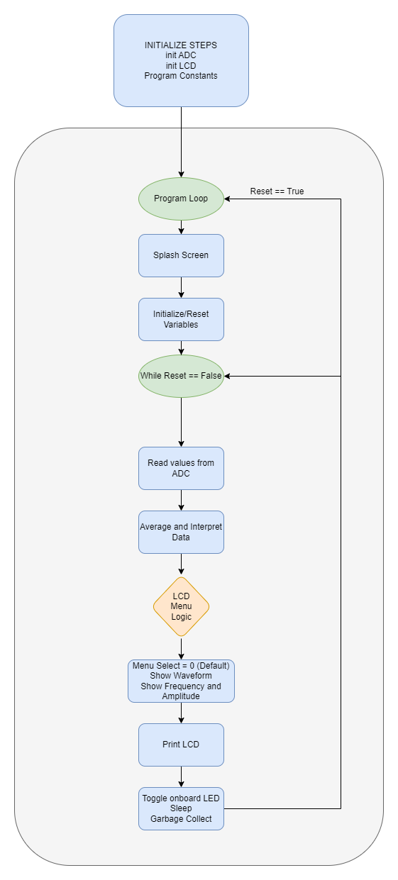
The Pico has a relatively simple program loop. A few systems such as the LCD and ADC are initialized on startup, then continuous readings from both ADC channels are taken for interpretation. Each channel has offset removed, becomes averaged over several samples, and scaled if necessary. Then the data is printed onto the LCD screen for interpretation. There are a few edge cases regarding the output being off, an open circuit, and a short circuit. In these situations, the LCD relays the situation to the user based on interpreted ADC data.
Schematic and PCB Design
All previously mentioned components must be compiled into a schematic design for wiring structure and PCB design. Bypass and decoupling capacitors are added to the board for several reasons. First, capacitors can be used on power headers to avoid voltage spikes and remove AC ripple on DC power. Small ceramic caps offer low series resistance and react fast but have a difficult time dealing with substantial amounts of charge over long periods. Polarized electrolytic capacitors usually have a much higher capacitance, and in conjunction with smaller ceramic capacitors, effectively clean DC voltage. In larger schematics and PCBs, we are not always able to position circuits near bypass capacitors. Therefore, small decoupling capacitors are recommended for placement near a circuit subsection to help clean AC ripple from DC voltages.
Once the schematic was populated with all necessary circuit components, the PCB was updated with all schematic components for board layout. A general layout of parts was done before resizing the board outline to find the most effective use of space. When all components have found their relative placement, routing traces for components using auto‑routing tools or manually is required. I chose to auto‑route, followed with manual edits to correct some trace routes. I found 100 mil routes were sufficient for this circuit. Copper pours are also recommended for adding a ground layer to the PCB, further simplifying routing design.
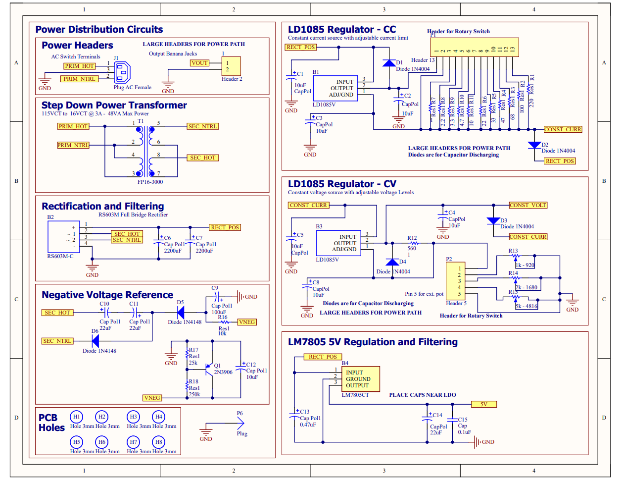 Power Supply schematic page 1 of 2
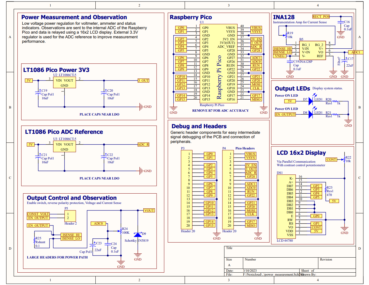 Power Supply schematic page 2 of 2
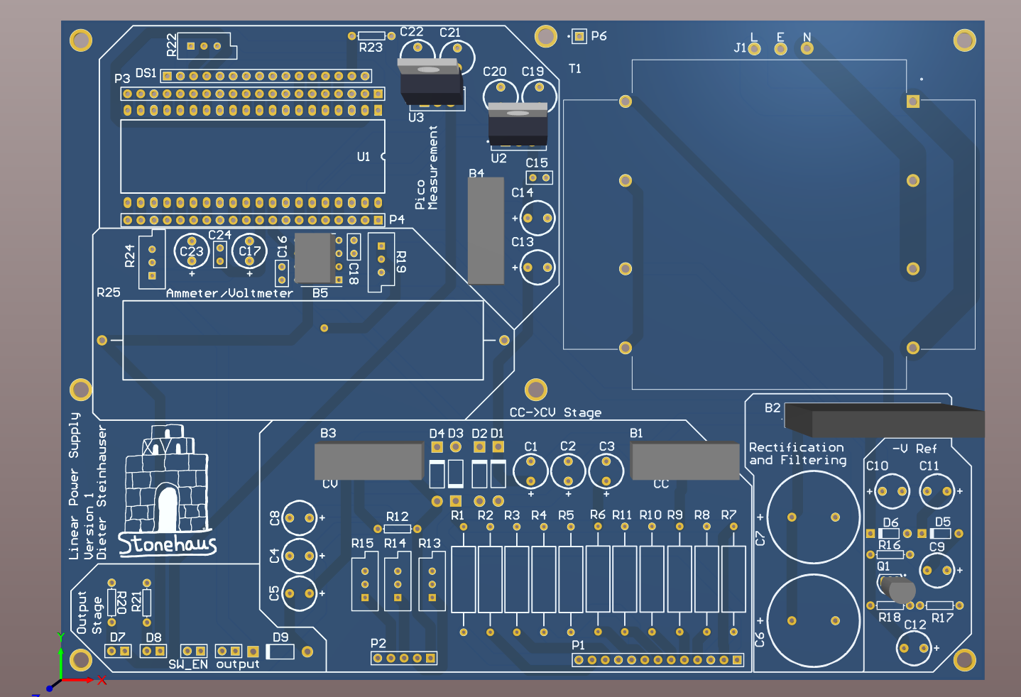 Top side of Power Supply PCB layout
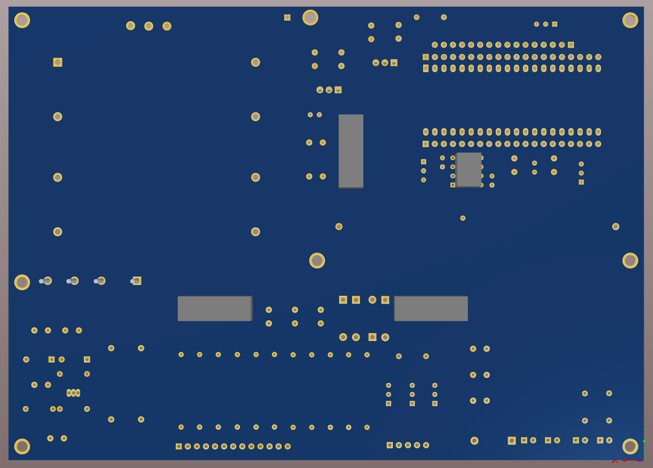 _Bottom side of Power Supply PCB layout
Results
The schematic of the circuit and PCB turned out fine, with a few errors that were fixable. The assembled PCB was easy to debug because of its plentiful headers employed in the diagram. Thankfully, there were no design‑breaking errors in this circuit, and most components worked immediately after installation.
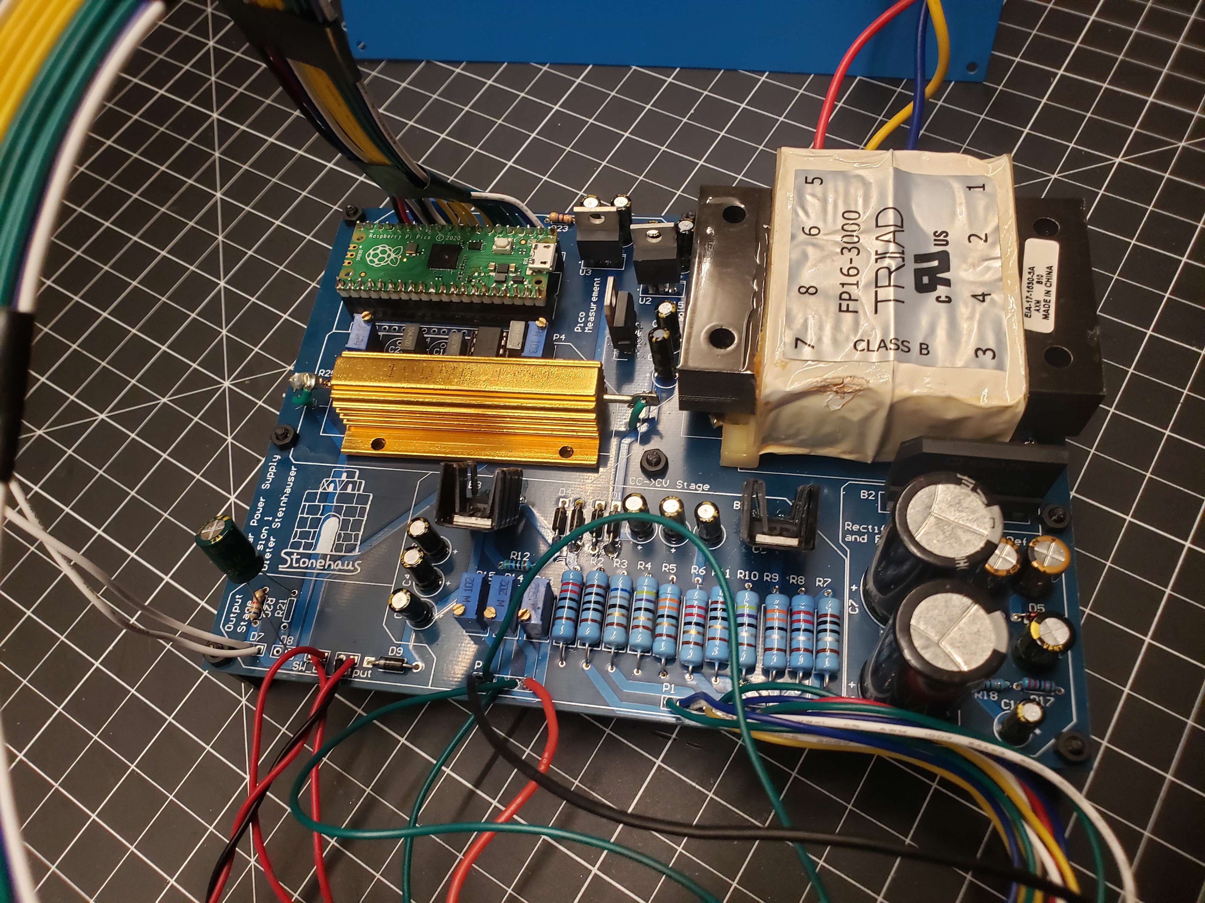 Power Supply Board
Flaws and Oversights
There were a few things that I messed up in designing the board, but acknowledging them is a good practice as lessons are learned and further revisions could be optimized. In terms of some minor design issues, I went overkill on a series of parts. The Raspberry Pico’s powerchain is excessive but works wonderfully. I could have easily removed one of the 3.3 V regulators and relied on the Pico’s internal SMPS fed from the 7805 for operation. This doesn’t affect the ADC since the reference is isolated from removing the R7 resistor. Using a linear regulator for an ADC reference was also overkill, and an LM385, TL431, or some other voltage reference could have been used to cut costs a bit. That being said, this powerchain worked wonderfully and provided very clean measurements.
In addition, I completely over‑specified the shunt resistor needed for current sensing. I employed a 100 W resistor thinking that the total power of the device could deliver 20 V × 3 A = 60 W during a short‑circuit condition. However, I neglected to see that the entire short‑circuit wire would act as a resistor and that the power dissipated on a resistance is equal to (I^2R) or about 1 W in my design. This is without mentioning any limiting or thermal shutdown that would occur.
Some more serious design errors included incorrectly wiring the instrumentation amplifier. This caused the device to read negative values and therefore send useless data to the ADC for current readings. Since I chose to use an IC riser, this was easily worked around using some wire wrapping. Some header ports were also too small for wires and made connecting the front panel difficult. The most egregious error was from designing the constant current regulator with decoupling capacitors and without a parallel limit resistor. These too factors led to the destruction of a handful of regulator ICs from current spikes.
Conclusion
Overall, this project has been insightful and a useful addition to my workbench. While there were some design faults, all errors were fixable and operation has not been impacted. Creating a linear power supply is a great way to introduce power electronics to engineers and provide utility to the engineer for future projects. This device performed well at providing power and realistic measurements to the user.
Appendix
main.py
1
2
3
4
5
6
7
8
9
10
11
12
13
14
15
16
17
18
19
20
21
22
23
24
25
26
27
28
29
30
31
32
33
34
35
36
37
38
39
40
41
42
43
44
45
46
47
48
49
50
51
52
53
54
55
56
57
58
59
60
61
62
63
64
65
66
67
68
69
70
71
72
73
74
75
76
77
78
79
80
81
82
83
84
85
86
87
88
89
90
91
92
93
94
95
96
97
98
99
100
101
102
103
104
105
106
107
108
109
110
111
112
113
114
115
116
117
118
119
120
121
122
123
124
125
126
127
128
129
130
131
132
133
134
135
136
137
138
139
140
141
142
143
144
145
146
147
148
149
150
151
152
153
154
155
156
157
158
159
160
161
162
163
164
165
166
167
168
169
170
171
172
173
174
175
176
177
178
179
180
181
182
183
184
185
186
187
188
189
190
191
192
193
194
195
196
197
198
199
200
201
202
203
204
205
206
207
208
209
210
211
212
213
214
215
216
217
218
219
220
221
222
223
224
225
226
227
228
229
230
231
232
233
234
235
236
237
238
239
240
241
242
243
244
245
246
247
248
249
250
251
252

# -----------------------------------------
#                 NOTES
# -----------------------------------------
"""
Dieter Steinhauser
12/2022
PicoPAD Test Script

"""

# -----------------------------------------
#               IMPORTS
# -----------------------------------------

from LCD import *
# import _thread
from utime import sleep, sleep_ms, sleep_us, ticks_ms
from machine import Pin, Timer, ADC, freq
# import gc

# -----------------------------------------
#         CONSTANTS/VARIABLES
# -----------------------------------------

# ------------------
REFRESH_RATE = 360 # Frequency in Hz
REFRESH_PERIOD = int((1 / REFRESH_RATE) * 1000) # delay in milliseconds

# ------------------
UPY_BIT_RES = 16
ADC_REF = 3.3
VOLT_PER_BIT = ADC_REF / (2**UPY_BIT_RES) # ADC recieves in 2 byte packets and micropython automagically fixes it.

# ------------------
DAC_REF = 5.0
DC_OFFSET = 0
DC_OFFSET_RES = int((DC_OFFSET / DAC_REF) * (2**UPY_BIT_RES))

# ------------------
FREQ_MAX = 160
FREQ_MIN = 10
AMP_MAX = DAC_REF
AMP_MIN = 0

MAX_DIST_US0 = 50
MAX_DIST_US1 = 20


# -------------------------------------------------------------
#           INITIALIZATION
# -------------------------------------------------------------

# -----------------------------------------
#           SYSTEM CLOCK
# -----------------------------------------

UNDERCLOCK = 30_000_000
DEFAULT_SYS_CLK = 125_000_000
STABLE_OVERCLOCK = 270_000_000

# Pico can go up to 270MHz before needing to flash to the eeprom directly.
system_clock = DEFAULT_SYS_CLK

# if the system clock is not the default, apply the clock speed.
if system_clock !=  DEFAULT_SYS_CLK:
    freq(system_clock)

# print(f'Clock: {freq()/1e6}MHz')

# -----------------------------------------
#               PINOUT
# -----------------------------------------

# LCD Pins handled in LCD.py
# ----------------------------
# EN = Pin(0, Pin.OUT)
# RS = Pin(1, Pin.OUT)
# D7 = Pin(2, Pin.OUT)
# D6 = Pin(3, Pin.OUT)
# D5 = Pin(4, Pin.OUT)
# D4 = Pin(5, Pin.OUT)

# Ultrasonic sensor pins handled in sensors.py
# ----------------------------
# us0_trig = Pin(6, Pin.OUT)
# us0_echo = Pin(7, Pin.IN)
# us1_trig = Pin(8, Pin.OUT)
# us1_echo = Pin(9, Pin.IN)

# Switches
# ----------------------------
# sw0 = Pin(10, Pin.IN, Pin.PULL_DOWN)
# sw1 = Pin(11, Pin.IN, Pin.PULL_DOWN)
# sw2 = Pin(12, Pin.IN, Pin.PULL_DOWN)
# sw3 = Pin(13, Pin.IN, Pin.PULL_DOWN)
# switch_pins = [sw0, sw1, sw2, sw3]

# LEDs
# ----------------------------
# led0 = Pin(14, Pin.OUT)
# led1 = Pin(15, Pin.OUT)
led_onboard = Pin(25, Pin.OUT)
output_en = Pin(16, Pin.OUT)
# led_pins = [led0, led1, led_onboard]

# SPI handled by the Hardware in spi_config.py
# ----------------------------
# miso = Pin(16, Pin.IN)
# cs = Pin(17, Pin.OUT, value=1)
# mosi = Pin(18, Pin.OUT)
# sck = Pin(19, Pin.OUT)

# Buttons
# ----------------------------
# button0 = Pin(20, Pin.IN)
# button1 = Pin(21, Pin.IN)
# button2 = Pin(22, Pin.IN)
# button3 = Pin(28, Pin.IN)
# button_pins = [button0, button1, button2, button3]

# ADC
# ----------------------------
# adc0 = ADC(26) # Connect to GP26, which is channel 0
# adc1 = ADC(27) # Connect to GP27, which is channel 1

# -----------------------------------------
#           LCD
# -----------------------------------------
lcd_init()
lcd_clear()
# lcd_cursor_on()
# lcd_cursor_blink()
# -----------------------------------------
#           ADC
# -----------------------------------------
adc1 = ADC(26) # Connect to GP26, which is channel 0
adc0 = ADC(27) # Connect to GP27, which is channel 1
# adc2 = machine.ADC(28) # Connect to GP28, which is channel 2
# adc_reading = adc0.read_u16() * VOLT_PER_BIT # read and report the ADC reading

# -----------------------------------------
#           SD CARD VIA SPI
# -----------------------------------------
#
# import sdcard
# import os
# import uos
#
# # Assign chip select (CS) pin (and start it high)
# cs = Pin(20, machine.Pin.OUT)
#
# # Intialize SPI peripheral (start with 1 MHz)
# spi = machine.SPI(0,
#                   baudrate=1000000,
#                   polarity=0,
#                   phase=0,
#                   bits=8,
#                   firstbit=machine.SPI.MSB,
#                   sck=Pin(18),
#                   mosi=Pin(19),
#                   miso=Pin(16))
#
# # Initialize SD card
# sd = sdcard.SDCard(spi, cs)
#
# vfs = uos.VfsFat(sd)
# uos.mount(vfs, "/sd")
#
# # Create a file and write something to it
# file = open("/sd/test01.txt", "w")
#
# with open("/sd/test01.txt", "w") as file:
#     file.write("Hello, SD World!\r\n")
#     file.write("This is a test\r\n")
#
# # Open the file we just created and read from it
# with open("/sd/test01.txt", "r") as file:
#     data = file.read()
#     print(data)

# -----------------------------------------
#           PROCESS 1: IO
# -----------------------------------------

while True:

    splash = True
    # Display the splash screen on startup.
    if splash is True:
        led_onboard(1)
        lcd_puts(f'Linear Supply   ')
        lcd_goto(0,1)
        lcd_puts(f'20V/3A Dieter S.')
        sleep(2)
        lcd_home()
        lcd_clear()
        led_onboard.toggle()

    list_length = 100
    counter = 0
    current_list = []
    voltage_list = []
    while True:

        # read ADC
        # -----------------------------------------

        adc0_reading = (adc0.read_u16() * VOLT_PER_BIT)
        adc1_reading = (adc1.read_u16() * VOLT_PER_BIT)

        voltage = (adc1_reading - 0.010) * 7.2962
        current = (adc0_reading - 0.010)

        current_list.append(current)
        voltage_list.append(voltage)
        counter += 1

        if counter == list_length:


            current = sum(current_list)/ len(current_list)
            voltage = sum(voltage_list)/ len(voltage_list)

            current = round(current, 3)
            voltage = round(voltage, 3)

            if current <= 0:
                current = 0

            if voltage < 0.9:
                voltage = 0
                current = 0
                output_en(0)
            else:
                output_en(1)

            counter = 0
            current_list = []
            voltage_list = []

            lcd_home()
            lcd_puts(f'A: {current}A       ')
            lcd_goto(0,1)
            lcd_puts(f'V: {voltage}V       ')

        # toggle onboard LED for System speed status and refresh delay
        # -----------------------------------------
        led_onboard.toggle()
        utime.sleep_ms(REFRESH_PERIOD)
        # gc.collect()