Texas Instruments Internship Experience
Design considerations for a buck converter's high-side gate driver.
Abstact
While working with the Texas Instruments (TI) Power Management IC (PMIC) group, I contributed to the analog design of a High-Side (HS) Gate Driver (GD) for a Low Voltage (LV), buck converter. I worked amongst a team of analog designers that specialized in DC-DC switching regulators, all of whom directly contribute to the cutting-edge PMIC product line offered by TI. For the three months I was present at Texas Instruments, I developed a deeper understanding of switching converters, device physics, circuit simulation, and semiconductor industry best practices. Leveraging this understanding, I revised existing TI intellectual property (IP) to update circuit bootstrapping, Break-Before Make (BBM) logic, and reinforce the block across PVT corners, all while targeting Automotive Safety Integrity Level D (ASIL D) compliance. This experience was beneficial for technical and professional growth, reinforcing knowledge from past classes while providing insight towards future class selection. Overall, my TI internship experience was positive, maturing my professional standing in electrical engineering, power electronics, and analog design.
Introduction
In the course of our academic career at the University of Florida, the pursuit of industry experience through internships is encouraged. Internships provide deeper understanding of knowledge gained at the university, perspective on course selection, networking opportunities, and professional development for career readiness post graduation. Taking a pause from my graduate studies, I joined Texas Instruments Power Management IC group for an internship in the summer of 2025. During my three-month term at TI, I was an analog design engineer contributing to a High-Side (HS) Gate Driver (GD) block within an integrated switch LV buck converter. The engineers within my PMIC analog design group develop DC-DC switching regulator blocks for multi-rail regulation ICs. While contributing to this project, I expanded my knowledge of step-down converters and device physics by analyzing existing buck high-side gate driver IP. My tasks included revising the previous design for new voltage domains, increased load current, and tighter performance constraints. This internship period provided opportunity to add significant value to a design, deepen my circuit mastery, and uphold TI values of professionalism.
Design
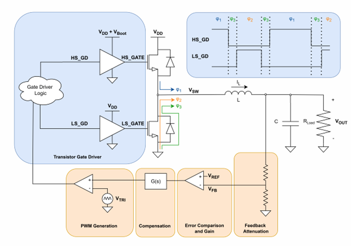 Figure 1: Synchronous rectifier buck converter topology.
Switching Converter Overview
The working principle of a step-down switching regulator is fairly simple. A reduced output voltage is generated during a given time period by averaging an input voltage switching between the supply and ground. Passive components such as inductors and capacitors create an average output voltage through low-pass filtering, tuned such that the switching frequency is rejected while the DC component passes 1. A combination of transistor and diode devices connect the switching node between the supply and ground. The system uses Pulse-Width Modulation (PWM) and feedback to control the switch node duty cycle and regulate the output voltage. Switching regulators such as the buck converter are beneficial due to their high-efficiency regulation. Assuming ideal, lossless devices, efficiency of switching regulators can reach 100%. However, non idealities such as conductive and switching losses occur which contribute to energy dissipation during system operation 1. Another drawback of switching regulators is the introduction of switching noise. While attenuated, switching harmonics at the output voltage are unavoidable. These factors poise switching regulators best for scenarios of high-efficiency energy transfer to load devices largely unaffected by transient noise, such as digital systems.
Buck Converter Operation
To operate the closed loop buck converter seen in figure 1, feedback from the output voltage is attenuated and compared against a known voltage reference, then compensated as needed for system stability before comparison against a triangle waveform to generate a PWM signal. Finally, the PWM signal triggers the transistor gate drivers to operate in a non-overlapping fashion and control the switching node voltage. Given the NMOS synchronous rectifier control of the switch node seen in figure 1, Three phases of switching operation will occur, where one of the devices are on by itself, or the low side body diode will conduct when both devices are off. Both switching FETs are NMOS due to higher carrier concentration, requiring the high side gate driver to supply a 𝑉𝐺𝑆 above 𝑉𝐷𝐷. Creating a voltage above the supply requires a bootstrapping circuit with a voltage multiplier or charge pump to dynamically generate the required voltage with small, on-chip capacitors.
 Figure 2: Example cross-coupled charge pump2
For example, figure 2 Illustrates a method of a cross-coupled FETs to switch between voltage boosting and charging states. Given the additional inversion between the capacitors, while one is boosted to the doubled supply, it activates the gate of the opposite device to charge the capacitor to the supply voltage and vice versa. Care should be exercised to have the charge pump non-overlapping, as overlap would cause drainage of the boosted voltage from the capacitor top through the FET to 𝑉𝐷𝐷. The architecture of figure 2 also requires a device tolerant to 2𝑉𝐷𝐷 or higher for safe operation of the output PMOS due to 𝑉𝐺𝑆 stress of 2𝑉𝐷𝐷.
Switching FET Adjustment
The design revision expected an increase from 2A to 4A DC load current, which required a lower 𝑅𝐷𝑆𝑂𝑁 for both high and low side switching FETs to maintain efficiency metrics and manage switching losses. Two main factors impact the 𝑅𝐷𝑆𝑂𝑁 for a FET, the gate to source voltage 𝑉𝐺𝑆, and the relative sizing of the device 𝑊/𝐿. While the gate voltage is determined by the gate driver architecture, the source voltage approaches the drain voltage due to the switch closing, making 𝑉𝐷𝑆 approach zero and reducing effective V𝐺𝑆. In terms of sizing, width can be increased for wider channel formation and therefore lower resistance current paths. Additionally, device length should be decreased or minimum, if the device length is not fixed. Thought should be given towards the Safe Operational Area (SOA) of the FET as well for a given length. Avoiding device degradation and breakdown by limiting applied 𝑉𝐺𝑆 and 𝑉𝐷𝑆 to the SOA specifications is a crucial design consideration. Otherwise, device width and the applied gate voltage are most influential towards meeting specifications, with the easiest adjustment being device width. As a result, a 2.5x magnification of the previous size was used to meet the target 𝑅𝐷𝑆𝑂𝑁, expecting the same 𝑉𝐺𝑆 applied.
Bootstrap Charge Sharing
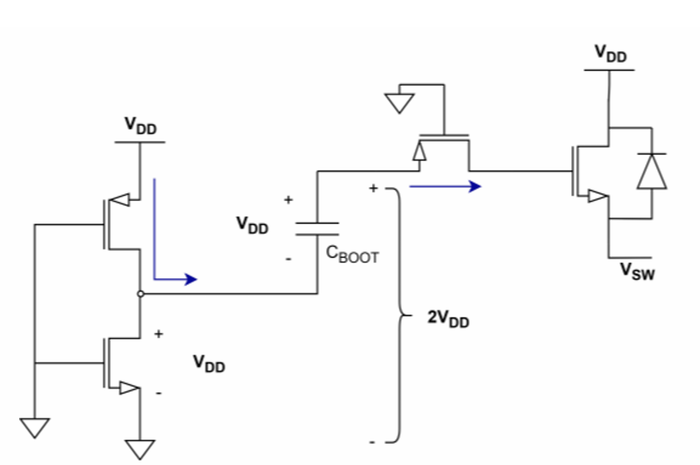 Figure 3: High-side gate driver in gate bootstrap phase.
 Charge sharing between the bootstrap capacitor and gate capacitance of the high-side switching FET
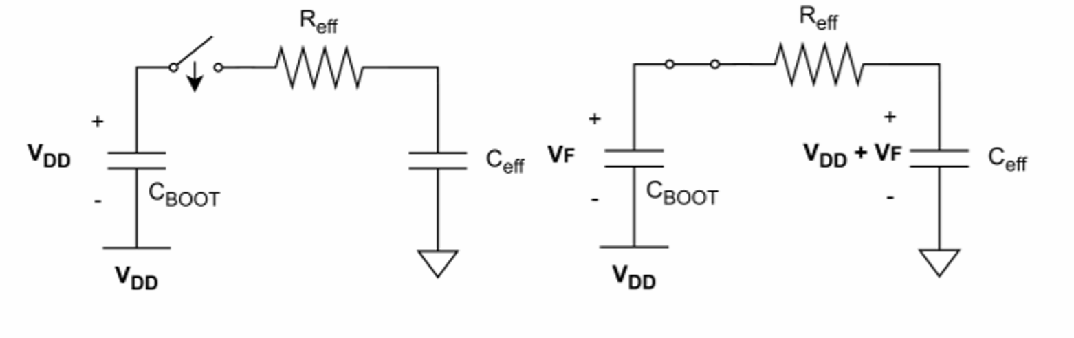
However, the increased area of the device results in higher gate capacitance, causing a larger load for the bootstrap circuit. Therefore, adjustment to the charge sharing circuit must occur to maintain the sharing efficiency and effective 𝑉𝐺𝑆. Charge sharing efficiency is determined by the voltage across the bootstrap capacitor after equilibration with the gate capacitance, as this is the potential difference of 𝑉𝐺𝑆 after the HS FET has closed and 𝑉𝑆𝑊 nears 𝑉𝐷𝐷. Presuming we use the circuit seen in figure 2 to feed the HS switch FET, we can simplify the phase of bootstrapping the HS gate to the circuit seen in figure 3. This showcases the voltage doubling effect and the active PMOS device allowing charge to accumulate at the HS FET gate. The circuit can be simplified further into figure 4, showcasing the equilibration of the two capacitances and the conduction loss over 𝑅𝑒𝑓𝑓. Response of the applied gate voltage directly correlates to the resistance of the series PMOS and gate capacitance. Since the gate capacitance grew, the resistance must shrink to match the previous IP’s RC time constant in the rising gate voltage. This is also necessary for maintaining efficiency as more current passes through the effective resistance. Additionally, the bootstrap capacitance must grow to maintain the capacitive ratio for equivalent 𝑉𝐺𝑆 . Neglecting resistive losses, estimation of final voltage across the boot capacitor can be determined by equation 1. Resistive losses can be best calculated by determining energy before and after equilibration, using equation 2.
\[\begin{equation} V_F = \frac{C_{boot}}{C_{boot} + C_{eff}} * V_{DD} \label{eq:1} \end{equation}\] \[\begin{equation} E = \frac{1}{2}CV^2 \label{eq:2} \end{equation}\]In practice, measuring 𝑉𝐹 / 𝑉𝐷𝐷 is sufficient for determining our efficiency. Propagation of our 2.5x size increase to the bootstrap capacitance, and a 3x increase in our PMOS pass transistor was sufficient to maintain performance of 88% charge sharing efficiency in the nominal case.
Parasitic Components and Device Stress
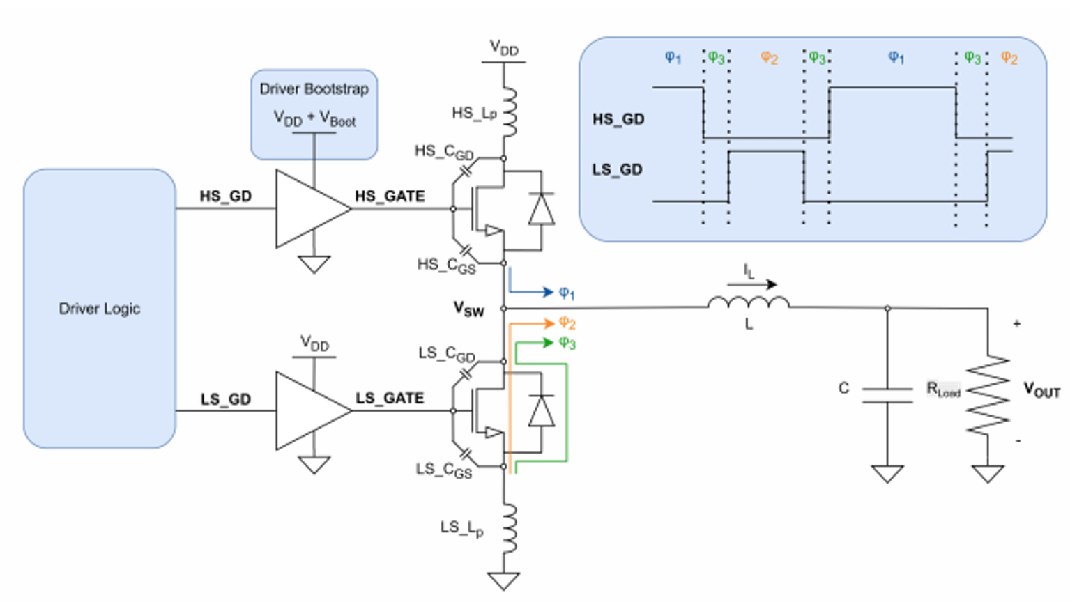 Figure 5: Synchronous rectifier buck converter with relevant parasitic devices.
Mitigation of inrush current, ringing, and device stress require a deeper understanding of parasitic circuit components and SOA. Parasitic inductance from PCB voltage sources have significant impact on buck converter operation, particularly on the HS FET due to 𝐶𝐺𝐷 and the miller effect. As the 𝑉𝐺𝑆 of the HS FET approaches 𝑉𝑇𝐻, The device enters the active region, acting as a common-source amplifier and magnifying the capacitance seen from gate to drain. Additional capacitance at the gate node slows down rise of 𝑉𝐺𝑆 forming the miller plateau while the 𝑉𝐷𝑆 falls 3. However, a slow rising edge also has benefits in dampening the LC step response. Since the rising edge of the HS gate occurs in phase 1 (blue), the body diode will enter reverse recovery after supplying 𝐼𝐿 current flow in phase 3 (green).
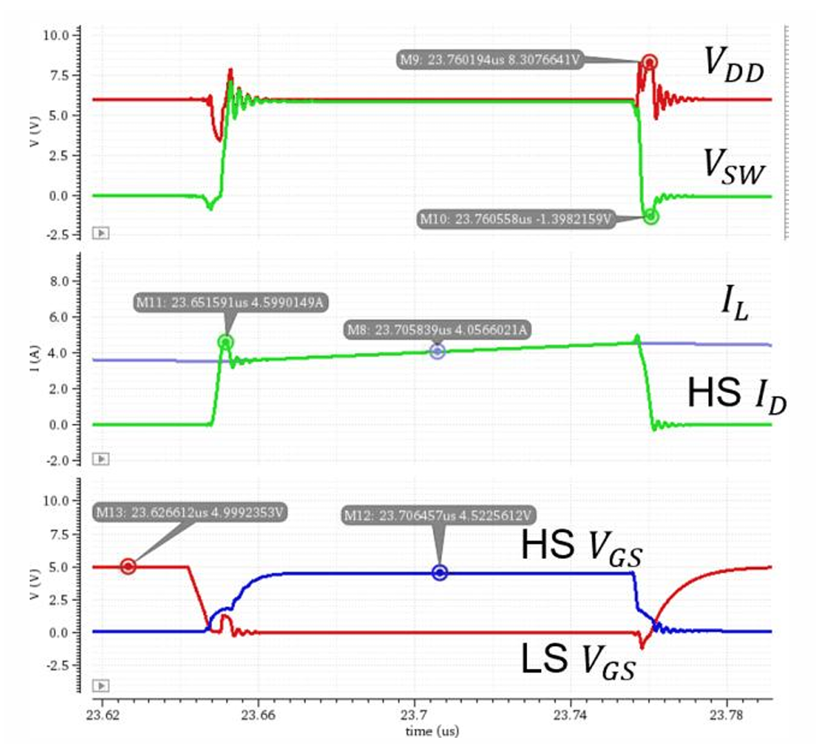 Figure 6: Synchronous rectifier buck converter steady-state simulation with parasitic devices.
Reverse recovery of the diode commands a large inrush current in addition to the constant inductor current, prompting an LC tank step response at 𝑉𝑆𝑊 and 𝑉𝐷𝐷. A careful balance of response time, feasible gate inrush current, and LC ringing must be found for safe and reliable operation.
Furthermore, upon the falling edge of the HS gate voltage, the HS FET experiences the highest 𝑉𝐷𝑆 stress due to LC tank ringing and 𝑉𝑆𝑊 snapping to a diode drop below ground in phase 3 (green). Device stress from high 𝑉𝐷𝑆 occurs due to Hot Carrier Injection (HCI), where the high potential difference will slingshot carriers across the channel and collide with atoms, causing impact ionization. This phenomenon ejects electrons, causing, damage in the gate oxide at the drain end, reducing current flow and trapping charges 4. Extreme stress can cause gate leakage current, breakdown through the gate oxide, or snapback through the bulk 5. While designs should obviously avoid device breakdown, impact ionization can be more insidious over the IC lifespan due to reduced current flow for a given 𝑉𝐺𝑆 applied to a FET. Maintaining the Gate Oxide Integrity (GOI) over the HS FET device’s lifespan is crucial for efficiency and current specification. Adjustment to the device switching characteristics can shape the LC step response and therefore the 𝑉𝐷𝑆 stress applied. Otherwise, consider widening the device to account for decreased current from deterioration over the expected lifespan. As a last resort, devices with larger safe operating areas may be used.
Break-before-Make and Edge Shaping
Insuring that the power switching FETs in the synchronous rectifier do not turn on at the same time is paramount for safe circuit operation. This non-overlapping period (phase 3, green) is generated intentionally to avoid a short circuit condition between the supply and ground. Digital logic feedback is utilized to notify one gate driver that the other has turned off, permitting the gate driver activation. Break-Before-Make (BBM) logic introduces propagation delay of a gate driver and the transitioning edge RC time constant as the time period of phase 3. Duration of phase 3 is likely asymmetrical when comparing intervals between active FETs due to differences in gate driver architecture from the high and low side, alongside differences in edge shaping. Regardless of FET activation interval, phase 3 describes current flow through the body diode of the LS FET. Miniscule durations of phase 3 across corners are desired for reduced conduction losses over the LS body diode. As a result, a balance of efficiency, driver propagation delay, and edge transition aggression must be found.
In other sectors of the architecture, BBM logic can be achieved without digital logic feedback. For example, creating non-overlapping operation of the charge pump circuit seen in figure 2. Voltage boosting of both capacitors simultaneously in an overlap period would cause leakage current. Charge would escape from the top of the capacitor to V𝐷𝐷 through the active NMOS. Since the timing difference in this scenario is a single inverter’s response, edge transitions can be shaped for slower rising and faster falling through device sizing.
Discussion
Design Considerations
Calculated design revisions on existing IP using the stated methods show similar performance to the previous design while maintaining stricter specifications for the operation lifetime. Changes to circuit voltage domains, non overlapping control logic, charge pump architecture, and gate bootstrapping permit similar operation. Timing, bootstrap efficiency, and the increased current load of 4A are maintained through the discussed changes. Steady state simulation across process, voltage, and temperature corners showcase operation of all systems within the margin of error.
Internship Takeaways
Overall, my experience with the TI PMIC group was positive and engaging. Exposure to the TI process node, chip planning, and analog design flow was deeply valuable towards readiness in a semiconductor industry. Professional growth was marked by a technical and interpersonal achievements. As an analog designer, I have a deeper understanding of physical limitations of devices, parasitic circuit components, and buck converter operation. As an engineer, I was emboldened to foster curiosity, engage in greater discussion, speak publicly with my team, and build a professional network.
Acknowledgment
My sincere gratitude towards my TI team for their support in my internship project. Their leadership and support have been instrumental in my success.
References
R. W. Erickson and D. Maksimović, Fundamentals of power electronics, Third edition. Cham: Springer, 2020. ↩︎ ↩︎2
R. J. Baker, CMOS: circuit design, layout, and simulation, 3rd ed. in IEEE series on microelectronic systems. Hoboken, N.J: Wiley, 2010. ↩︎
P. Horowitz and W. Hill, The art of electronics, Third edition. Cambridge, New York: Cambridge University Press, 2024. ↩︎
P. R. Gray, Analysis and design of analog integrated circuits, 5. ed. Hoboken, NJ: Wiley, 2010. ↩︎
T. C. Carusone, D. Johns, K. W. Martin, and D. Johns, Analog integrated circuit design, 2nd ed. Hoboken, NJ: John Wiley & Sons, 2012. ↩︎